인텔 Ravi Mahajan, EMIB 칩 패키징 기술 개발 인터뷰
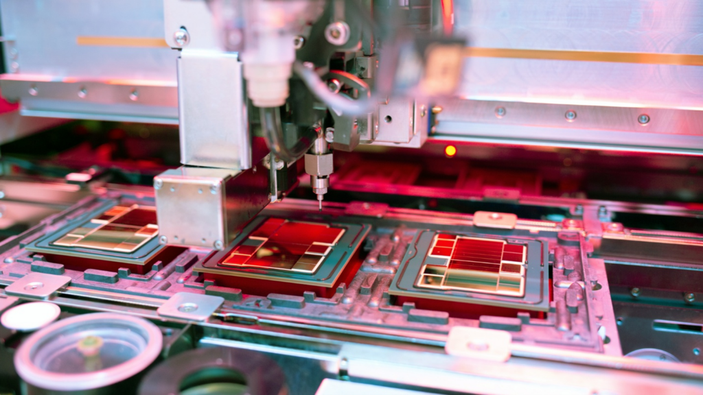
무슨 발표인가
- —EMIB 개발자 Ravi Mahajan이 반도체 패키징 30년 이상 경력 보유
- —EMIB 기술로 다중 칩을 단일 패키지에 밀착 연결
- —AI 워크로드의 고성능·대역폭·에너지효율성 요구 대응
원문 (영어)
Meet the Intel Pioneer Behind EMIB Chip Packaging May 28, 2026 Published Intel Foundry Hide Show Image --> Ravi Mahajan discusses the idea for a simple silicon bridge and why it is becoming a foundational technology for the AI era. --> Share In this article: Ravi Mahajan is a foundational figure behind Intel’s leadership in advanced packaging.
As an Intel Fellow and director of Substrate and Advanced Packaging Pathfinding at Intel Foundry , he has spent more than 30 years advancing semiconductor packaging technologies. Often referred to as the inventor of EMIB (Embedded Multi-die Interconnect Bridge), Mahajan led the development of this groundbreaking technology that enables multiple chips to be tightly interconnected within a single package, an increasingly important capability as AI workloads drive demand for higher performance, bandwidth and energy efficiency.
In this conversation, he reflects on his career, the origins of EMIB, the growing importance of advanced packaging, and why system-level innovation is becoming central to the future of computing. Q: Why is advanced packaging increasingly at the center of global technology conversation?
For decades, the semiconductor industry relied on transistor scaling—what we often refer to as Moore’s Law—to drive performance improvements. At the same time, demand for compute has accelerated dramatically, especially with AI. These workloads require not just more compute, but significantly higher memory bandwidth, and energy efficiency especially in managing the data traffic.
Advanced packaging has emerged as a critical new lever. It allows us to bring multiple chips together in a highly integrated way, enabling system-level performance gains that would not be possible through monolithic scaling alone.
원문: Intel Newsroom — "Meet the Intel Pioneer Behind EMIB Chip Packaging" (2026-05-28) 공식 원문: https://newsroom.intel.com/intel-foundry/meet-the-inventor-of-emib