엔비디아-TSMC AI, 반도체 설계·제조 고도화
무슨 발표인가
- —NVIDIA CUDA-X·AI 모델로 리소그래피·트랜지스터·공정 시뮬레이션 가속화
- —NVIDIA Metropolis·TAO로 결함 검사 자동화
- —반도체 설계부터 양산까지 전 단계 최적화
원문 (영어)
News Summary: NVIDIA CUDA-X libraries and AI models are accelerating TSMC workloads across lithography, transistor and process simulation, advanced process control and fab operations optimization. TSMC is using NVIDIA Metropolis and NVIDIA TAO Toolkit to advance automated defect inspection with vision AI, improving detection of nanometer-scale defects while reducing repeated labeling and retraining.
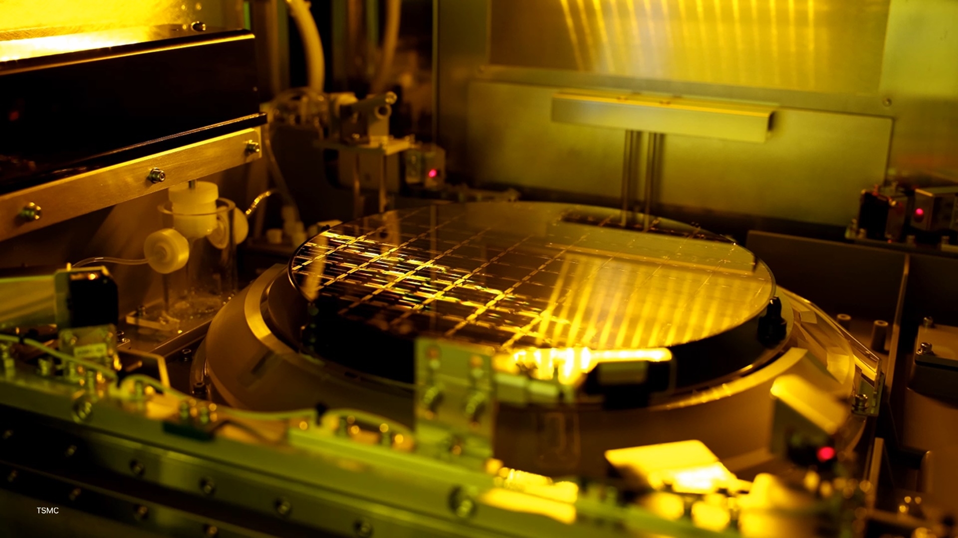
NVIDIA GTC Taipei — NVIDIA today announced that TSMC, the world’s leading semiconductor company, is using NVIDIA accelerated computing and AI to advance semiconductor design and manufacturing. As chips move to more advanced nodes, bringing them from design to high-volume production has become one of the world’s most complex computing challenges.
Computational lithography, transistor simulation, process control and wafer inspection now require massive-scale simulation and real-time optimization, and AI systems that can provide support across physics, images and other applications. TSMC is using NVIDIA technologies to accelerate this transformation, applying accelerated computing and AI across the semiconductor design and manufacturing lifecycle to improve turnaround time, energy efficiency, yield and operational productivity in advanced fabs.
“NVIDIA and TSMC have worked together for nearly three decades to push the limits of computing,” said Jensen Huang, founder and CEO of NVIDIA. “TSMC is bringing NVIDIA AI and accelerated computing into the fab itself, tackling some of the world’s most complex design and manufacturing challenges with simulation, optimization and AI to improve speed, efficiency and yield for the next generation of chips.”
원문: NVIDIA News — "NVIDIA and TSMC Bring AI Into Fabs to Advance Semiconductor Design and Manufacturing" (2026-06-01) 공식 원문: https://nvidianews.nvidia.com/news/nvidia-and-tsmc-bring-ai-into-fabs-to-advance-semiconductor-design-and-manufacturing